3D Print PCBs (3D Printed Circuit Boards) – All You Need to Know

3D printing PCBs can enable faster, cheaper, and more innovative PCB design, but can it resolve the electronics industry’s supply issues? Let's take a look.
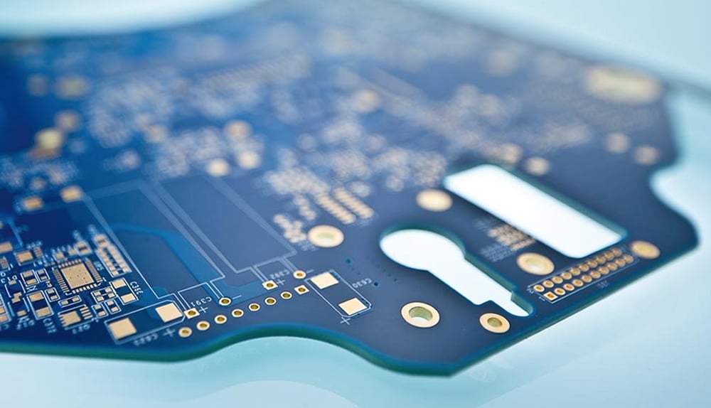
3D printed circuit boards are faster to make than traditional production methods, more versatile, and can provide significant cost savings while producing more complex circuits. For rapid prototypes, low-volume production, and unique electronic products (especially for military or aerospace applications), 3D printing offers electronics manufacturers a path to producing circuit boards in-house faster and cheaper than outsourcing fabrication.
Another appeal of 3D printed PCBs today is that they give manufacturers the critical ability to control their circuit board supply and eliminate disruptions from plant shutdowns, shipping slowdowns, or geopolitical maneuvering; all of which have stretched circuit board supply chains to the breaking point leaving manufacturers scrambling for alternatives.
This technology is still a relative niche, and more R&D is needed to scale it to mass-production levels, but recent advancements have already allowed manufacturers to disrupt traditional electronics manufacturing enabling accelerated speed to market for new products. One 3D printer maker Optomec, for example, says its semiconductor solution increases 5G signals by up to 100%.
There are more reasons why manufacturers have been quick to embrace 3D printed PCBs. Here we look at the 3D printers that can make circuit boards, the software used to design 3D PCBs, and other ways additive manufacturing is making an impact in the circuit board industry, such as how additively manufactured tools and fixtures are used in PCB production. We also explore who’s using 3D PCBs today and services where you can get your boards printed.
What Are 3D Printed Circuit Boards?
3D PCB technology is a relative newcomer to the electronics industry, but it has advanced rapidly in recent years.
Specialized circuit board 3D printers can manufacture boards much faster than conventional methods, and for some applications, you can even use a common desktop FDM 3D printer with conductive filament.
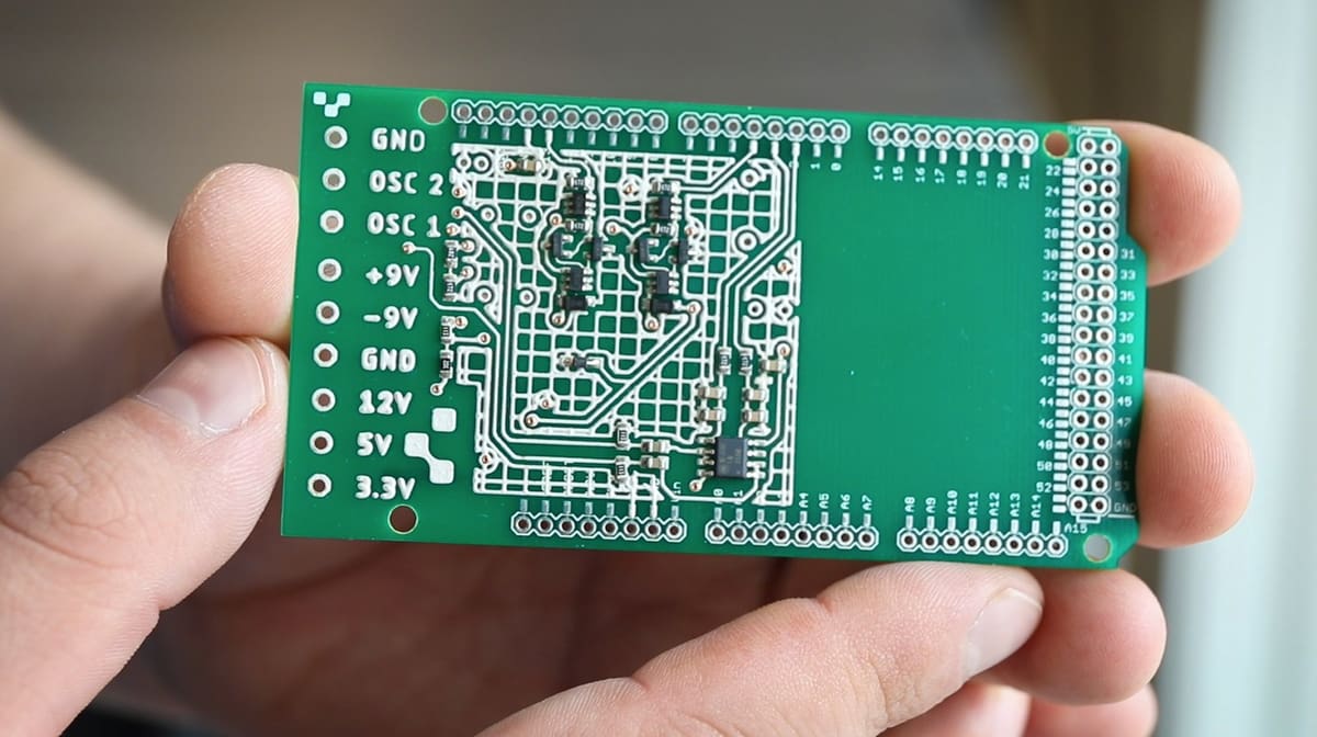
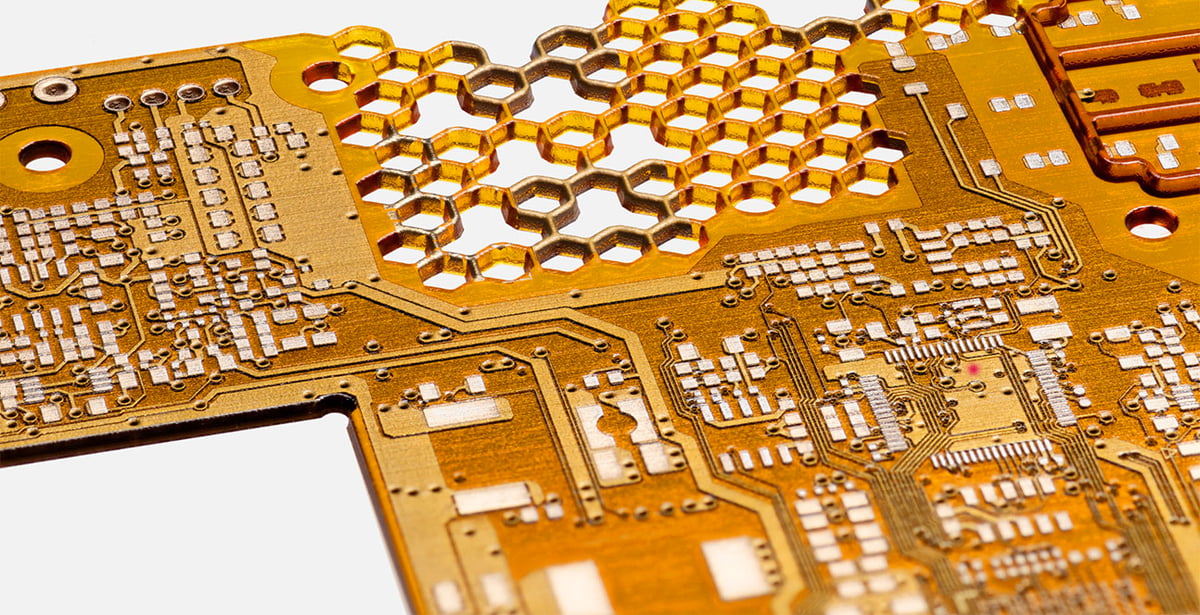
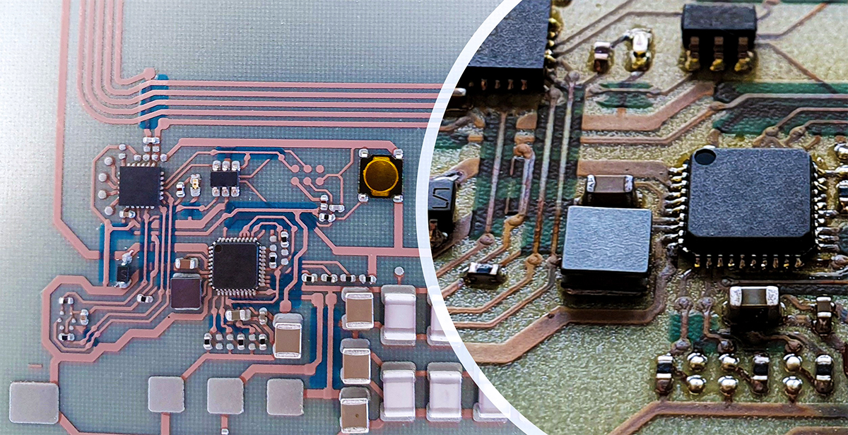
Whereas a traditional circuit can take days or months to produce, 3D printers can create a functional circuit board in less than 24 hours. Design freedom is another significant factor. 3D printers can create circuits in shapes much more complex than the traditional rectangular board, including flexible boards, honeycomb structures, and even fully three-dimensional boards.
PCB 3D printing technologies generally work in two ways: printing the circuitry directly with conductive materials or printing a circuit board with hollow channels or trenches that are later filled with conductive materials. Let’s take a closer look at what sets these methods apart.
Circuit board 3D printers construct the entire board through additive manufacturing. It stands apart from some old PCB production methods, which use mechanical means to etch circuitry onto a board or simply CNC mill conductive traces.
Method 1: Conductive Materials
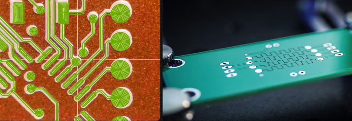
Conductive materials are probably the kind of 3D printing you’d expect to see when hearing the term “3D printed circuit boards.” These types of PCB 3D printers lay down a conductive material to form the circuitry. These materials usually come as inks or filaments infused with conductive particles, such as silver, copper, or graphite. These materials can also be sprayed as an aerosol-laden stream of material.
Inks are the more common option in commercially available PCB 3D printers. They use inkjets similar to those found in 2D printers to deposit droplets of both conductive and insulating ink to build the circuitry. Some printers need a prefabricated substrate board, while others can print the entire board from scratch. In the latter case, the printers can produce complex, multilayered, and double-sided circuit boards with embedded components, such as coils, resistors, or LEDs.
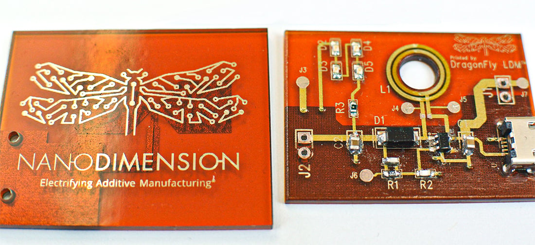
One example is a 10-layer 3D PCB with high-performance electronic structures soldered to both outer sides. Using a dielectric polymer ink and conductive ink from Nano Dimension, Hensoldt, a German-based sensor manufacturer specializing in the defense industry, 3D printed boards that are conductive and insulating simultaneously.
Conductive filaments are another option for printing circuit boards. You can print these filaments with practically any FDM printer, which makes them more cost-effective. However, the circuitry will be bulkier and most likely less efficient than ink-based PCBs. As such, conductive filaments may not be suitable for commercial operations, but they are ideal for prototypes.
Method 2: Hollow Traces
The second method produces a circuit board with hollow channels where the circuitry will be. Essentially, you’ll be printing a “case” to hold the conductive material you deposit into the channels after printing. For the circuit to function, you’ll have to print the board with a non-conductive filament, like ABS or PLA.
This method enables you to create PCBs with virtually any sufficiently accurate 3D printer. It can therefore be a very economical solution. It can also provide higher conductivity than some directly printed circuits, particularly those made with conductive filaments.
For example, PCB maker Beta LAYOUT relies on a selective laser sintering machine from EOS to 3D print circuit carriers conductor tracks that are later filled with conductive material.
Pros and Cons of 3D Printed PCBs
3D printing PCBs can provide significant advantages over conventionally manufactured circuit boards, but it also has some very real limitations. Therefore, it may not be an ideal technology for all purposes, just yet.
Pros
- Cost-efficiency: Although some PCB 3D printers are costly, they can quickly make a return on the investment. 3D printed PCBs consume fewer materials to produce. Additionally, eliminating shipping and outsourcing costs can make circuit prototyping significantly cheaper.
- Production Speed: With 3D printers, PCB production time is counted in hours, not days. They can speed up the entire pipeline, from circuit design, prototyping, and iteration, to end-use production and market rollout.
- Design Freedom: PCBs produced with 3D printers can be practically any shape, and it’s also possible to print them with flexible materials. With higher design freedom, engineers can concentrate on making products lighter, smaller, and more efficient.
- Less Waste: Traditional production methods can produce a lot of waste while also requiring you to leave unnecessary space on the board, which further wastes resources. 3D printed PCB can make circuits more compact with complex shapes, which saves material. Not only will you save money, but you may also be able to use the low-waste angle in your marketing.
- On-Demand Production: 3D printing enables you to produce circuit boards as needed without keeping large inventories. At the same time, you won’t have to commit to large orders from third-party manufacturers, while also eliminating the chance of supply chain disruption.
- High Accuracy: 3D printers can achieve higher accuracies in PCB production than traditional methods. Some printers can even place components, further reducing the possibility of human error in the production process.
- More Layers: Your board geometry can be more complex when you use an additive manufacturing system for high layer count PCBs.
Cons
- Limited Materials: As a relatively new technology, 3D PCB printing doesn’t yet have an extensive range of suitable materials. Many printers are locked to one or two materials from their manufacturer, which can increase costs and limit design choices. On the other hand, some printers, just as the nScrypt boast a palette of more than 10,000 commercially available materials.
- Lower Conductivity: Although PCB 3D printing is constantly advancing, some conductive printing materials don’t perform as well as traditional ones.
- Limited Board Size: 3D printers can only produce PCBs as large as their print chamber allows (which isn’t an issue for most applications). As many PCB 3D printers have rather small print chambers, they’re unsuitable for producing large circuit boards.
- Lack of Options: Just like with materials, there are currently few companies manufacturing PCB 3D printers commercially. This situation is highly likely to improve as the technology matures, but for the time being, you don’t have a wide range of options to choose from.
Applications of 3D Printed Circuit Boards
3D PCBs have already built several convincing cases for uses. Manufacturers have successfully produced PCBs for applications in various industries, from education to advanced aerospace devices.
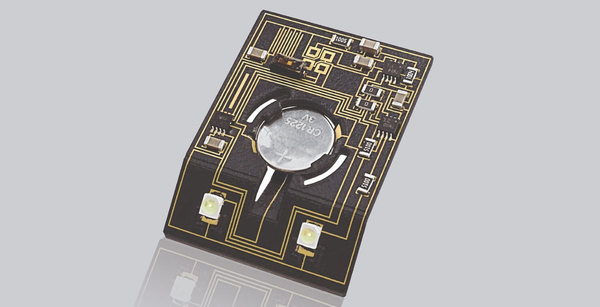
3D PCBs for Biomedical Research
The Bao Research Group at Stanford University in California is developing new alternative electronics, such as flexible and biocompatible ones. For example, Dr. Naoji Matsuhisa, a postdoctoral researcher, is developing stretchable sensors for next-generation biomedical wearable devices.
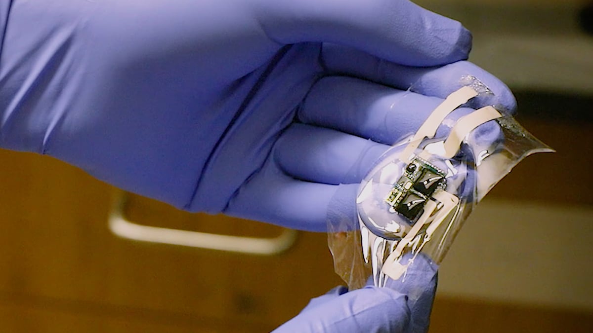
The sensors for many of the devices are deposited on stretchy, extremely flexible substrates to get them as close to the skin as possible. These sensors must then connect to a rigid circuit board. The connection point, however, must also stretch to allow for comfortable wear and the highest degree of functionality. Bao Research uses Voltera’s V-One 3D printer to produce stretchable conductors for the connecting components.
“Previously, we have used screen printing masks or some sensor printing masks, but the feedback is very slow,” explaines Dr. Matsuhisa. Additionally, the kinds of structures the Bao group needs are difficult to produce using conventional PCB production methods. The V-One allows the Bao Research Group to manufacture the unusual circuitry and connectors they need quickly.
3D Printing Solar Cells for Renewable Energy
The Fraunhofer Institute for Solar Energy Systems ISE is a German-based research center that performs scientific and engineering research and development to advance solar and photovoltaic power production technology. They use Optomec’s aerosol jet (AJ) 3D printing system to production solar cells on Fz wafers. The 3D printing technology enables Fraunhofer ISE to print fine-feature collector lines between 18 and 60 microns in width using silver-infused inks. This seed layer is then covered in a surface layer consisting of multiple conductive materials.
The 3D printed solar cells have a higher conductivity and a lower shadowing effect than previously used cells. As a result, the technology has helped Fraunhofer ISE to increase its solar cells’ efficiency by 20%. Following the technology’s success, multiple commercial solar cell manufacturers have adopted the technology to develop more effective solar cells for green energy production.
Aerospace & Military
Phased array antennas are complex arrays of antenna elements that allow operators to change their radiating patterns without physically moving the antenna. This is possible by controlling the phase of each antenna element’s signal so it can be “aimed” at a specific spot — like a laser beam compared to a lightbulb. These devices are critical in both aerospace and military applications to facilitate secure communications.
Florida-based engineering company Sciperio, working in partnership with the U.S. Air Force Research Laboratory (AFRL) successfully developed a method to print complex, multilayer RF electrical structures on curved surfaces. This enables the company to produce phased antenna arrays for aircraft and other aerospace and military applications.
The key to the project’s success was the nScrypt 3Dn Series Factory in a Tool (FiT) 3D manufacturing system. Combining FDM 3D printing with microdispensing, aerosol jetting, and component placement, the 3Dn FiT system enables Sciperio to manufacture the complex structural electronics necessary for the curved antenna array.
Radio Frequency Communications
L3 Harris Technologies, a global aerospace and defence technology corporation headquartered in Melbourne, Florida is using 3D printed technology to radically change how radio frequency (RF) systems are manufactured. RF technology includes amplifiers used in radio and television broadcasting, wireless communication, and radar systems, and can be highly complex and expensive to produce.
With the help of 3D printers, L3 Harris is hoping to change that. As part of their Space and Intelligence Systems department, Senior Scientist, Dr. Arthur Paolella believes, “The ability to manufacture RF systems in house offers an exciting new means for rapid and affordable prototyping and low-volume manufacturing.”
Specifically, the company looked into ways to manufacture a circuit board with two types of packaging incorporated in it – one rigid and one flexible. In addition, they wanted it built fast and economical, with no extra cables or connectors. What they were able to create using the DragonFly Pro System, was a high functioning circuit board about the size of a credit card in less than 10 hours. The PCB had no recognizable difference in either input or output response loss response when tested for certain frequency ranges, nor was there a significant difference measured in gain when compared to circuits built using traditional methods. This has the possibility to significantly reduce the cost and production time in the future.
3D Printed PCBs: State of the Art
R&D into 3D PCBs is taking place on a range of fronts for various industry sectors. Below are some of the most promising developments.
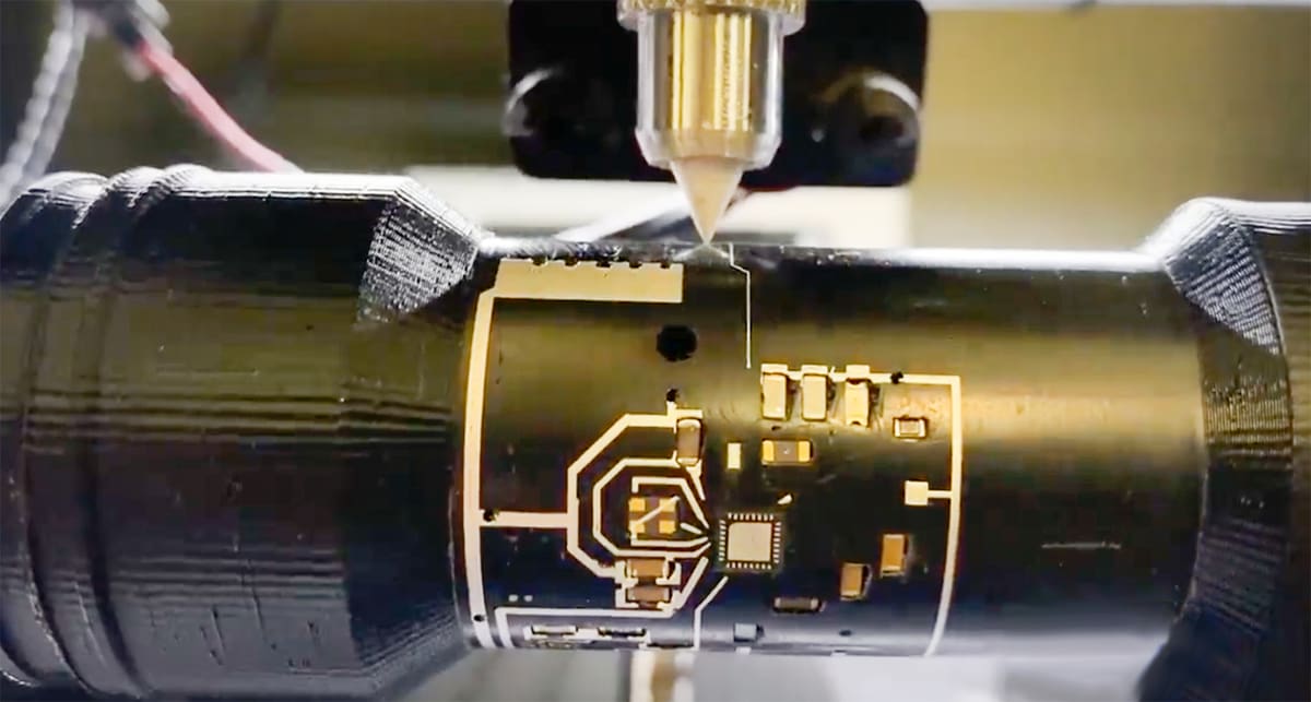
Not Just Boards, Printing Circuits on Any Shape
One significant development — demonstrated at the 2022 IPC APEX Expo, the major PCB conference — is moving beyond circuit boards and into printed circuit structures (PCS).
Engineers are realizing that they’re no longer restricted to flat boards and can instead make circuits in practically any shape. For example, a 3D printed circuit cylinder was among the demonstrations at ICP APEX. These new shapes can help manufacturers fit PCBs into smaller spaces and produce them at a lower price. Although this technology isn’t yet ready for commercialization, it shows the direction the industry is evolving.
Meanwhile, researchers at the University of Houston announced in June 2022 that they’d created a new type of 3D printable resin infused with organic semiconductor materials. With the resin, the research team successfully printed such objects as micro-printed circuit boards. This discovery could pave the way for small, bioactive electronics that could be used in wearable sensors, prosthetics, implanted neural chips, and other medical appliances.
Additive PCB Manufacturing to Replace Etching Processes
In August 2022, a partnership between German companies InnovationLab and ISRA VISION reported they’d achieved a breakthrough in 3D PCBs. The duo created a functioning physical prototype using novel 3D printable copper ink. The multilayer PCB is compatible with conventional reflow soldering, allowing manufacturers to mount components without purchasing any new equipment.
“This is a state-of-the-art production process, which will decrease costs and reduce logistical dependencies on suppliers while delivering three key benefits for the environment: consuming fewer materials, using less energy, and producing less waste. By the end of [2022], we expect to have scaled this process to high volumes, meeting customer demands of a million solderable tracks or more,” said Dr. Janus Schinke, InnovationLab head of printed electronics.
The InnovationLab 3D PCB uses substrates that are up to 15 times thinner compared to conventional techniques, which reduces material consumption and means the production process has less waste.
Top Circuit Board 3D Printers
Compared to more established 3D printing technologies, the 3D-printed PCB market is currently quite small. But despite its niche status, there are multiple machines available to choose from. Here are a few highlights of currently available PCB 3D printers.
Nano Dimension DragonFly IV
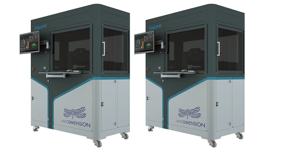
Introduced in 2015, Nano Dimension’s DragonFly was touted as the world’s first desktop-sized 3D printer for producing professional-grade PCBs. The company’s current offering — the DragonFly IV — doesn’t fit on a desk, but it’s nonetheless a powerful solution for AME production.
DragonFly IV deposits two specialized inks onto the printing bed. The first of them is AgCite, an ink filled with conductive pure silver nanoparticles. AgCite provides PCBs with predictable conductivity even at a 75-micron layer height. The second ink consists of a dielectric polymer, which provides structure and insulation for the PCB at layer heights as small as 18 microns.
DragonFly IV deposits these inks simultaneously and cures them using infrared and ultraviolet light. The printer can create high-performance devices and circuits, even with complex three-dimensional shapes. Starting the print jobs is easy with Nano Dimension’s Flight software, which integrates seamlessly with DragonFly IV. Flight enables users to control everything from data preparation and printability verification to the actual print process.
DragonFly IV is also powered by DeepCube, Nano Dimension’s proprietary AI solution for additive manufacturing. Using the same principles as speech or image recognition AI, DeepCube improves part quality and output by identifying defects too tiny for the human eye to see and correcting printing errors in real-time. Connected to 3D printers worldwide, DeepCube learns to be more efficient and accurate with each print run.
In addition to DragonFly IV, Nano Dimension offers the Fabrica 2.0 micro 3D printer, which can serve electronics manufacturers by creating miniature connectors and other tiny components.
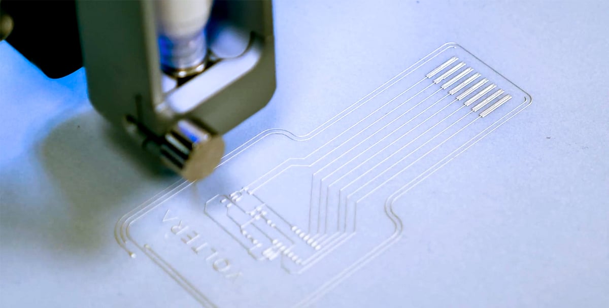
Voltera Nova & V-One
Ontario-based Voltera launched its latest 3D printer for electronics in October 2022. The new Nova is designed to 3D print on soft, stretchable, and conformable electronics as well as rigid boards. It’s an evolution of the company’s previous V-One 3D printer. The Nova enables users to create smart devices on their benchtop, the company says, and features a modular design to expand.
Voltera’s still offers its popular V-One PCB 3D printer that puts its emphasis on ease of use and fast production. It’s an affordable machine that isn’t beyond the budgets of even small and medium-sized businesses.
V-One provides an all-in-one PCB production package. It’s capable of dispensing conductive ink, drilling holes into circuit boards, and heating and curing ink and reflow. Each of these tasks is carried out by a different head. Voltera has made switching the head easy — the magnetically mounted heads pull off and snap on in seconds without any tools.
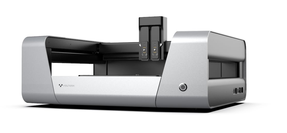
Instead of printing the entire board, V-One relies on either pre-fabricated or pre-printed boards. Although you have to either purchase or print boards separately, you can choose their material freely, as V-One is substrate agnostic. Voltera offers both standard and flexible conductive inks, enabling users to print PCBs for a wide range of applications.
After placing the board into the printer, V-One aligns the print head height and begins depositing the conductive ink before finally curing it. The machine works quickly and can produce a simple single-layer PCB in 2-3 hours. V-One can currently produce two-layer boards, but Voltera hopes to add further multi-layer support in the future.
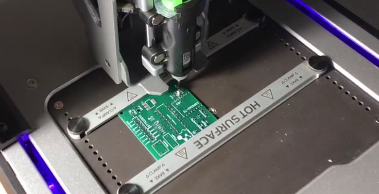
BotFactory SV2
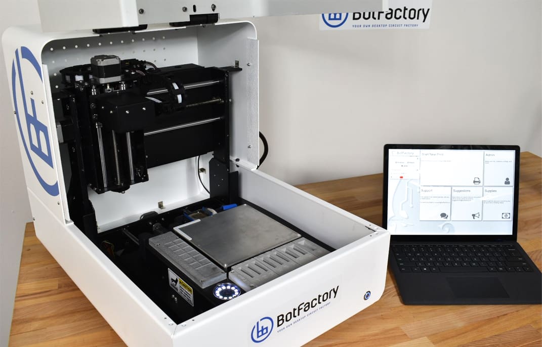
BotFactory’s first PCB printer, the adorably named Squink, came out in 2015, competing with Nano Dimension’s DragonFly for the title of the first desktop PCB printer. The Squink has now been discontinued and BotFactory has replaced it with the more professionally-oriented SV2.
BotFactory touts SV2 as an all-in-one desktop printer, aimed particularly for research and engineering applications. The machine can print multilayered circuits with conductive and insulating inks, deposit solder paste, place components as small as 0603 resistors on the board, and finally cure the inks and reflow the solder paste.
In addition to conductive and resistive inks, BotFactory has created a resistive ink for SV2. This material allows manufacturers to directly print resistors onto PCBs, removing the need to install separate resistor components. Users can create flexible PCBs without worrying about detaching parts, create resistors with specific values, or create embedded components with SV2.
The printer is available as a Starter, Enhanced, and Professional version. The Starter and Enhanced models can print a maximum of two layers while the Professional model is capable of creating four-layer PCBs. The min clearances with the printer models range from 400 microns to 300, and 200, respectively.
nScrypt 3Dn Series FiT
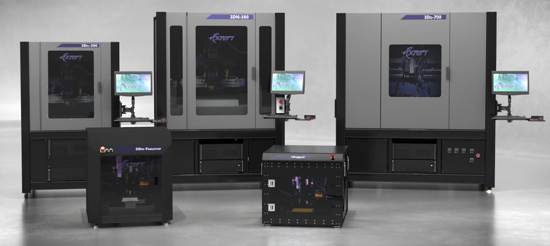
Although many PCB 3D printer manufacturers market their machines as all-in-one circuit board printers, nScrypt claims its 3Dn Series Factory in a Tool (FiT) system goes even further. According to the manufacturer, this solution wraps an entire small factory into one package.
The FiT machines are equipped with an FFF 3D printer, but they’re also capable of microdispensing, drilling, polishing, and placing components with 1-5 exchangeable tool heads (or gizmos as the manufacturer calls them). With automatic tool changes, post-processing methods, and a claimed support for more than 10,000 materials, the 3Dn Series FiT machines are suitable for manufacturing products, not just parts, nScrypt says.
The FFF printing and microdispensing functionalities are of particular interest to PCB producers. With the FiT machine, it’s possible to 3D print a device’s structure and housing while also dispensing embedded conductive traces as thin as 20 microns. This allows the production of what nScrypt has dubbed Printed Circuit Structures — 3D-printed objects with circuitry embedded within them.
The 3Dn Series FiT printers are available in both tabletop-sized and gantry platform models.
Optomec Aerosol Jet Flex
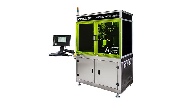
New Mexico-based Optomec has created a unique solution for additively manufacturing PCBs and other electronics. Dubbed Aerosol Jet (AJ), the technology enables printing conductive traces on both 2D and 3D substrates. According to Optomec, AJ can create interconnects in 2D applications that emulate multi-layer circuit boards on a single layer by making use of dielectric material at circuit crossover points. The technology can also print circuitry directly on 3D surfaces without the need for wire bonding.
Optomec’s flagship machine is the Aerosol Jet Flex 3D printer. It can be configured to have three to five axes of motion and can print features as small as 10 microns and layer heights down to 100 nanometers. The printer also has a well-sized print chamber for a PCB 3D printer, with a maximum build volume of 350 x 250 x 300 mm.
Electronics manufacturer Lite-On Mobile uses the technology to 3D print antennae onto mobile phones, and Optomec says its machines are installed at Samsung, Lockheed Martin, GE, and several undisclosed military customers.
AJ Flex uses an atomizer to turn its ink-based materials into a dense aerosol mist. The mist is delivered onto the printing platform through a deposition head, where a sheath gas focuses the aerosol into a highly targeted beam. This method enables printing circuitry on plastic, ceramic, or metallic substrates.
Optomec offers a variety of add-on modules for AJ Flex. The laser sintering module enables room temperature sintering of metal inks, while the UV curing module allows operators to cure UV-sensitive polymers to create 3D structures. The wide-feature print head, as the name implies, unlocks extended printed feature sizes up to 2800 microns.
Nano3Dprint B3300
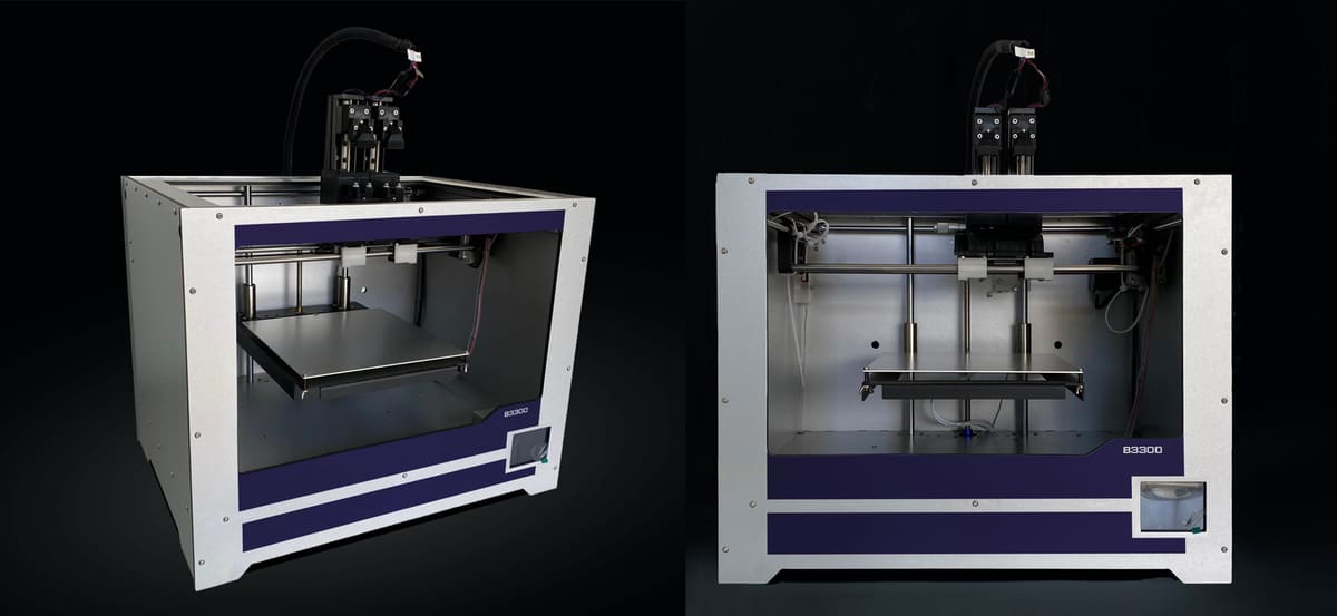
The B3300 Dual-Dispensing 3D printer for electronics from California-based Nano3Dprint can print 3D patterns onto any substrate and combine materials, such as conductive inks, gold, silver, UV-curable polymers, and silicone to create wearables and functional electronics with embedded circuitry.
The technology enables incorporating sensors, strain gauges, heaters, complex antenna geometries, and optical components in a 3D print, the company says, and provides manufacturing solutions for the medical, agriculture, and solar industries, and general consumer electronics.
The printer features a video inspection system that allows users to monitor their progress while being small enough to fit on a desktop. It is compatible with most CAD or slicer software and retails for $6,000.
For those in the market for printing on a much smaller scale – and have a much larger budget, Nano3Dprint is offering the D4200S for preorder sales. This new printer prints on the micro to nano scale, with a 50 nanometer print resolution. Geared towards commercial use, this printer can be reserved with a 25% minimum down payment – roughly $62,500.
Circuit Board 3D Printing Services
PCB 3D printers can require a significant upfront investment that may not suit all budgets. Fortunately, it’s possible to get PCBs 3D printed without purchasing a machine of your own. PCB 3D printing services allow you to order PCBs for prototyping and end-use purposes. They’re also a great way to try the technology before committing to a purchase.
Nano Dimension
In addition to manufacturing the DragonFly 3D printer, Nano Dimension offers PCB design and fabrication services. The company operates printing labs around the globe, enabling it to offer turnaround times counted in days. Nano Dimension engineers can also work with clients to design and customize PCBs and high-performance electronic devices from scratch to fit various applications.
Beta Layout
Beta Layout specializes in 3D printing and manufacturing PCB prototypes. Combining its two areas of expertise, the company offers 3D Mechatronic Integrated Device (3D-MID) prototyping services. Beta Layout can 3D print complex objects with integrated circuitry. Its technology enables the miniaturization of electronic components and allows manufacturers to prototype innovative circuit structures faster than with traditional production methods.
Phytec New Dimensions
Phytec New Dimensions, a subsidiary of the aforementioned Phytec, offers PDB 3D printing using Nano Dimension’s DragonFly technology. The company focuses on producing proof-of-concept PCBs and offers both assembled PCBs and individual design studies to determine a project’s feasibility for 3D printing. Phytec promises fast turnaround times, with a completed prototype printed in two working days.
Software for Circuit Board Design
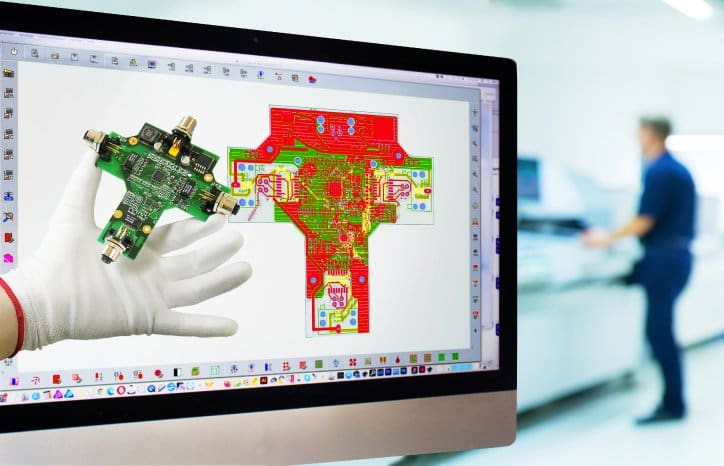
Designing and making PCBs open up new avenues for everyone from hobbyists to small businesses. Design software is the first step. Even a simple PCB requires a multitude of parameters to be collated: component lists, physical layouts, interconnection paths, physical dimensions, and much more. PCB design software helps designers manage all of this by efficiently visualizing the entire design process.
For more sophisticated, even multilayer, PCBs, you’ll need a more robust solution like these below. But do they 3D print your circuit boards? If you want to 3D print PCBs or the enclosures for your PCBs, you need additional software such as a standard MCAD application or a mesh file generator. Most of the 3D printer companies mentioned above offer software to convert your design into a format specific to the 3D printers.
We cover the top software products in our updated guide linked below:
License: The text of "3D Print PCBs (3D Printed Circuit Boards) – All You Need to Know" by All3DP Pro is licensed under a Creative Commons Attribution 4.0 International License.